
Isolated Analog-to-Digital Conversion
Isolation components, such as the ACPL-C799, allow you to transfer data without establishing a direct electrical connection between two parts of a system.
Galvanic isolation is an important design technique when one portion of a circuit must be separated from the voltages or currents in another portion of the system. Actually, though, galvanic isolation by itself is not complicated—just don’t establish a conductive path between the two sub circuits. The trick is moving electrical information between these sub circuits.
If we can’t share data via electricity, we need to use something else. A typical approach is the use of light (though other options are available). However, optical coupling can become a bit unwieldy when you’re dealing with multiple digital signals. If you have an eight-bit parallel data bus, a direct implementation would require eight separate LED-plus-optical-detector circuits.
So let’s say you have an analog signal in one portion of your circuit, and you want to digitize this signal and pass the data to another portion. Simple enough, but what happens when these two subcircuits must be galvanically isolated? We don’t want a 16-bit parallel-output ADC that will lead to an interface consisting of 16 optocouplers.
A much more reasonable approach is to digitize the signal in a way that results in fewer digital interconnections, and the natural choice in this case is sigma-delta modulation:

All images (unless otherwise noted) are taken from the ACPL-C799 datasheet.
Here we have a conversion scheme that maps the analog input voltage to a certain density of logic-high vs. logic-low states. The result is a one-bit output signal that, despite its single-bittedness, can represent conversion resolutions that are quite impressive. (A quick Digi-Key search indicates that sigma-delta ADCs currently offer resolution as high as 32 bits.)
The Integrated Approach
As always, you don’t have to do much design work to implement fully isolated analog-to-digital conversion. Chips like the ACPL-C799 can handle the details:

As you can see, the ACPL-C799 incorporates analog signal processing, sigma-delta modulation, and the optical-coupling interface. The output consists of the sigma-delta digital signal and the corresponding clock signal (the frequency is 10 MHz, and note that it’s generated internally—no oscillator required).
The Filter
You might be wondering, though: What am I supposed to do with this logic-high-density signal? It’s a fair question; generally we want our ADC data in the form of (digital) numbers.
Well, it turns out that you actually do need some circuitry in addition to the ACPL-C799 if you want typical ADC data. To be more specific, you need a decimation filter; this signal-processing block converts the one-bit data stream into typical multi bit data, and at the same time it reduces the sampling rate. The datasheet recommends a sinc filter, and it also notes that you can use an FPGA or a digital signal processor for this task (if you aren’t fortunate enough to have a DSP or an FPGA in your system—well, you’ll have to get creative).
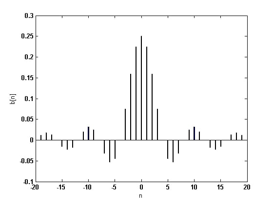
A discrete impulse response based on a sinc function (image borrowed from this article).
The exact nature of the final ADC data depends on the characteristics of the filter, not on the ACPL-C799 itself. The datasheet gives an example in which the filter has a decimation ratio of 256 and is designed for 16-bit output data. This will result in a sample rate of (10 MHz)/256 ≈ 39 kHz and an ADC resolution of (you guessed it) 16 bits.
The Analog Side
The ACPL-C799’s analog input range—positive 80 mV to negative 80 mV—is quite small, so you might need a voltage divider (and then a buffer) to ensure that your input signal is compatible. The following table gives you an idea of how different input voltages correspond to the sigma-delta data and the filtered ADC data.

Also, you will note that the datasheet specifies a “linear” input range of ±50 mV, not ±80 mV. Yet the table reproduced above clearly indicates a ±80 mV range. What is the datasheet trying to tell us here? Answer: I don’t know!
As far as I can tell, the analog input circuitry is fully functional at voltages up to ±80 mV, but linearity performance diminishes beyond ±50 mV. The datasheet states enigmatically that the analog input stage accepts voltages of “±50 mV (full scale ±80 mV).” Elsewhere it insinuates that there’s something not so good about voltages beyond ±50 mV because ±50 mV is the “recommended input range” (emphasis mine). All I can say is be careful—if you want to push your input signal up toward ±80 mV, there may be consequences.